Introduction
Semiconductor fabrication facilities face contamination challenges where even trace volatile compounds from O-rings can cause significant yield loss. Research shows that O-ring degradation in process environments leads to particle formation, metallic contamination, and volatile organic compound (VOC) deposition that directly impacts wafer quality and device performance.
Cleanrooms operating under ISO Class 5-7 standards must control contamination at the molecular level. A single O-ring releasing condensable volatiles can fog optical lenses in lithography tools, deposit films on wafer surfaces during CVD processes, or introduce mobile ions that compromise device reliability.
Those failures translate directly to scrap wafers, equipment downtime, and millions in lost production — which is why material selection and outgassing compliance are non-negotiable in these environments.
This article covers the technical requirements that separate semiconductor-grade O-rings from industrial seals:
- Outgassing mechanisms and measurement (TML, CVCM, WVR)
- Material selection across FFKM, FKM, and silicone families
- SEMI standards compliance and testing methodologies (ASTM E595, IEST protocols)
- Specification practices that reduce contamination risk
Key Takeaways
- Key outgassing thresholds per ASTM E595: TML below 1.0% and CVCM below 0.10%
- FFKM perfluoroelastomers offer lowest outgassing and broadest chemical resistance for critical plasma etch, CVD, and vacuum applications
- Material purity covers volatile release, particle generation, ionic contamination, and metal content
- ISO Class 5-7 manufacturing and DI water cleaning (>18 MΩ·cm) prevent surface contamination before installation
- Application-specific validation beyond standard testing ensures materials perform under actual process conditions
What Outgassing and Purity Represent in Semiconductor Cleanroom O-Rings
Outgassing is the release of trapped volatiles, residual monomers, plasticizers, cure by-products, and adsorbed gases from elastomeric materials when exposed to vacuum, elevated temperature, or aggressive chemical environments. Unlike bulk material properties, outgassing represents a contamination pathway that becomes critical in semiconductor manufacturing where sub-micron particles or molecular films cause defects.
When O-rings outgas in process chambers, released compounds deposit onto wafer surfaces, optical components, chamber walls, and mix with process gases. This contamination causes multiple failure modes: haze on lenses that degrades lithography resolution, particle defects that create circuit shorts, film contamination that alters electrical properties, and equipment performance degradation.pdf) requiring costly cleaning cycles or component replacement.
Purity requirements encompass two distinct but related characteristics:
- Outgassing properties measure volatile release — a time-dependent phenomenon highest during initial vacuum exposure that decreases with bake-out and conditioning
- Material cleanliness reflects inherent characteristics set by formulation and manufacturing: extractables, ionic contamination, particle shedding, and metal content
Both must be controlled to prevent contamination.
That distinction matters because standard test data doesn't always predict real-world behavior. Published outgassing values typically reflect ASTM E595 conditions (125°C, 10⁻⁵ Torr, 24 hours) — but a material that passes screening can still contaminate when exposed to plasma etching, thermal cycling, or corrosive gases that accelerate degradation well beyond initial test predictions.
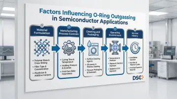
Factors That Influence Outgassing and Contamination in Real-World Semiconductor Applications
Material Formulation
Base polymer selection sets the ceiling for chemical resistance and thermal stability. From there, every formulation choice either introduces or limits contamination risk:
- Peroxide cure systems produce fewer extractables than sulfur-based alternatives
- Plasticizers and processing aids must be minimized or eliminated — these low-molecular-weight additives outgas readily
- Filler type and loading determine particle generation risk
- Stabilizer packages prevent degradation but can become contamination sources if poorly selected
Manufacturing Process Controls
How an O-ring is made directly affects how clean it arrives:
- Cure temperature and time must be sufficient — insufficient cross-linking leaves residual monomers
- Post-cure protocols drive off volatiles before the O-ring reaches the cleanroom
- Mold release agents must be cleanroom-compatible or fully removed before shipment
- Production in ISO Class 5–7 cleanrooms prevents particle contamination at the source
Cleaning and Packaging
Even a well-made O-ring can be compromised before it enters the tool. Proper handling includes:
- DI water rinse at >18 MΩ·cm resistivity to remove particles, residual mold release, and water-soluble contaminants
- Vacuum packaging promptly after cleaning to prevent re-contamination from atmospheric particles and moisture
- Double-bagging with cleanroom-certified materials for transport and storage protection
Operating Environment
In-process conditions often exceed what standard outgassing tests simulate:
- High vacuum (<10⁻⁶ Torr) drives more aggressive volatile release than rough vacuum (10⁻³ Torr)
- Thermal cycling generates particles through repeated expansion and contraction at sealing surfaces
- Plasma exposure with RF power and reactive chemistry (NF3, CF4, O2) etches O-ring surfaces, producing degradation products that standard tests don't capture
- Corrosive gas, solvent, and dopant exposure attacks polymer chains directly
Service History
Contamination risk evolves across an O-ring's service life. The first vacuum exposure releases the highest volatile load. Re-outgassing occurs each time the chamber vents to atmosphere, as the elastomer reabsorbs moisture and airborne contaminants. Over time, degradation products from chemical attack or plasma etching accumulate — making proactive seal replacement essential before catastrophic process failure.
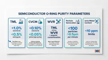
Critical Purity Parameters and Their Acceptable Ranges
Semiconductor O-ring purity is governed by SEMI S2 environmental guidelines, SEMI S8 safety standards, customer specifications, and application-specific contamination budgets that vary by process tool and device node.
Total Mass Loss (TML)
TML measures the percentage of mass lost when material is exposed to vacuum at elevated temperature per ASTM E595: 24 hours at 125°C under 5×10^-5 Torr vacuum. All volatile species released — including water vapor — are captured in this measurement, making TML a conservative total outgassing metric.
Typical semiconductor requirement: TML <1.0% (NASA low-outgassing standard). More stringent applications requiring ultra-high vacuum or sensitive optical systems specify TML <0.5%. High-purity FFKM compounds typically achieve TML values of 0.2-0.5% based on manufacturer testing data, while standard industrial elastomers often exceed 2-3%.
Collected Volatile Condensable Materials (CVCM)
CVCM measures the percentage of volatiles that condense on a cooled collector plate (25°C) during ASTM E595 testing. Unlike TML, which includes non-condensable gases and water vapor, CVCM specifically quantifies species that will deposit as films on cooler surfaces.
Typical semiconductor requirement: CVCM <0.10%. Ultra-high purity applications (lithography optics, wafer-facing surfaces in deposition chambers) require CVCM <0.05%. This parameter directly predicts contamination risk for sensitive surfaces — higher CVCM values correlate with faster lens hazing and film buildup on chamber walls.
Water Vapor Regained (WVR)
WVR measures the percentage of mass regained when material is exposed to humid air (50% RH) after the outgassing test. This represents moisture absorption capacity and helps distinguish water loss from organic volatile loss.
The formula TML − WVR = non-aqueous outgassing reveals the true organic contamination potential of a material:
- High WVR, low (TML − WVR): Material primarily releases absorbed water, which evaporates without leaving organic residue
- Low WVR, high TML: Material releases organic volatiles that deposit as sticky films on surfaces
Additional Purity Metrics
Three additional metrics round out a complete purity profile:
- Particle generation (per IEST-STD-CC1246): Requires <100 particles >0.5μm per minute under agitation, simulating dynamic seal operation to catch shedding from surface abrasion or filler migration
- Ionic contamination: Extractable ions (Na+, K+, Cl⁻, F⁻) measured by ion chromatography; mobile ions migrate through dielectric layers under electrical bias, causing reliability failures — limit typically <10 ppm total extractable ions
- Metal content (via ICP-MS): Transition metals (Fe, Cr, Ni, Cu, Zn) cause device defects at trace levels; standard requirement is <10 ppm total metals, with stricter limits (<1 ppm) for high-concern contaminants like copper or sodium
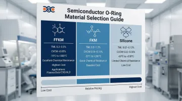
Material Selection Criteria for Low Outgassing Semiconductor O-Rings
No single elastomer excels across every dimension. Effective selection means matching a material's specific strengths — outgassing performance, chemical resistance, temperature range, and mechanical behavior — to the actual demands of the application.
Perfluoroelastomers (FFKM)
FFKM is the premium choice for semiconductor sealing. It delivers the lowest outgassing of any common elastomer — TML typically 0.2–0.5%, CVCM <0.05% — and resists the full range of process chemicals: fluorinated plasmas, strong acids and bases, aggressive solvents. Temperature range runs -15°C to 300°C continuous, with specialty grades tolerating brief excursions to 327°C. Full performance data is available in the Trelleborg Isolast product guide.
FFKM runs 10–20× more than FKM, but that cost premium pays off in critical applications: vacuum chamber lid seals, plasma etch tool process kits, CVD reactor gas distribution systems, ALD chamber seals, and lithography equipment where contamination directly affects yield.
Compound formulation matters as much as material class. Specify semiconductor-grade low-outgassing formulations rather than general-purpose FFKM developed for chemical processing — the latter often contains process aids that compromise purity.
Fluoroelastomers (FKM/Viton)
FKM provides cost-effective performance for less critical applications. Low-outgassing grades achieve TML 0.5–1.5%, CVCM 0.05–0.15% — adequate for many semiconductor applications but not matching FFKM purity. Chemical resistance handles many wet chemicals and moderate vacuum service. Temperature capability spans -20°C to 200°C.
Always specify low-outgassing, low-compression-set formulations — not standard commercial grades. FKM compounds formulated for automotive or general industrial use contain plasticizers and process aids that cause unacceptable outgassing and particle generation in semiconductor environments.
Suitable applications include roughing pump seals, chemical delivery systems for less aggressive chemistries, lower-vacuum chambers (>10⁻⁴ Torr), and non-plasma environments where chemical exposure is moderate.
Silicone Elastomers (VMQ, FVMQ)
Silicone offers extreme low-temperature flexibility (-60°C) and specific biocompatibility characteristics useful for medical device semiconductor components. Standard silicones have poor outgassing performance and chemical resistance, but cleanroom-processed, low-volatile grades can meet semiconductor requirements when specified correctly.
Specialty grades achieve TML 0.07–0.12% and CVCM 0.02–0.05% — strong outgassing performance — according to Parker Chomerics test data. Chemical resistance remains limited compared to fluoroelastomers, though fluorosilicone (FVMQ) improves on standard VMQ while retaining low-temperature capability.
Material Selection Decision Framework
Start with process conditions:
- Vacuum level: High vacuum (<10⁻⁶ Torr) demands lowest outgassing; rough vacuum (10⁻³ Torr) allows broader material options
- Temperature range: Continuous operating temperature and thermal cycling extremes
- Chemical exposure: List all process gases, cleaning chemicals, and solvents
- Plasma environment: Yes/no, and if yes, RF power and gas chemistry
Evaluate contamination sensitivity:
- Wafer-facing seals require strictest purity (CVCM <0.05%, particle generation <50/min)
- Optical path seals need low CVCM to prevent lens hazing
- Non-critical locations (sub-fab, exhaust lines) allow relaxed specifications
Consider seal design constraints:
- Compression set resistance for static seals maintaining long-term sealing force
- Hardness requirements for surface finish compatibility
- Dimensional stability under thermal cycling
Optimize for cost-effectiveness:
- Reserve FFKM for applications where its unique properties justify premium cost
- Use properly formulated FKM where chemical and thermal demands allow
- Consider silicone for low-temperature or specialized applications
| Material | TML (%) | CVCM (%) | Temp Range (°C) | Chemical Resistance | Relative Cost | Typical Applications |
|---|---|---|---|---|---|---|
| FFKM | 0.2–0.5 | <0.05 | -15 to +300 | Excellent (all chemicals) | 10–20× | Plasma etch, CVD, ALD, critical vacuum |
| FKM | 0.5–1.5 | 0.05–0.15 | -20 to +200 | Good (most chemicals) | 1× (baseline) | Chemical delivery, rough vacuum, non-plasma |
| Silicone | 0.07–0.12 | 0.02–0.05 | -60 to +200 | Limited (select chemicals) | 0.8–1.5× | Low-temp, biocompatible, static seals |
Testing, Specification, and Validation Methods
Testing serves both material qualification (verifying vendor claims) and ongoing quality control. Semiconductor applications require multiple validation layers beyond standard material property testing.
Industry Standard Test Methods
ASTM E595 is the primary outgassing test method, exposing materials to 24 hours at 125°C under 5×10^-5 Torr vacuum. The test provides TML, CVCM, and WVR values that form the basis for NASA low-outgassing certification. This screening test identifies materials suitable for vacuum service but doesn't predict long-term contamination behavior.
ASTM E1559 (contamination outgassing test) measures outgassing kinetics and deposition rates over time using Quartz Crystal Microbalances. This advanced method models contamination accumulation on sensitive surfaces, predicting when optical components require cleaning or when chamber walls need maintenance. The kinetic data reveals whether outgassing decreases rapidly (acceptable) or continues at problematic rates (unacceptable for long service intervals).
SEMI S2 (Environmental, Health, and Safety Guideline for Semiconductor Manufacturing Equipment) addresses material safety and contamination control, establishing expectations for material compatibility and environmental impact. SEMI S8 focuses on ergonomic design but references S2 for broader safety considerations.
Cleanroom Manufacturing and Cleaning Validation
Semiconductor-grade O-rings should be manufactured in ISO Class 5-7 cleanrooms (equivalent to Fed Std 209E Class 100-10,000) with controlled temperature, humidity, and particulate levels. Manufacturing in controlled environments prevents particle contamination during molding—a critical control point since surface particles can't be completely removed by subsequent cleaning.
DI water cleaning with resistivity >18 MΩ·cm removes surface particles, residual mold release, and water-soluble contaminants. Suppliers validate cleaning effectiveness through three methods:
- Particle count testing per IEST-STD-CC1246
- TOC analysis (Total Organic Carbon) measuring organic contamination in final rinse water
- Visual inspection under magnification for surface defects or residues
Double-bagging in cleanroom environment immediately after cleaning prevents re-contamination during storage and transport. Inner and outer bags should be cleanroom-certified materials, sealed in controlled environment.
Material Certification and Traceability
Material certifications provide documented evidence of purity and performance. Essential documentation includes:
- ASTM E595 test reports with actual TML/CVCM values for the specific compound (not just "meets NASA low-outgassing")
- Material composition disclosure identifying base polymer and major additives
- Lot traceability enabling quality investigations when contamination events occur
Suppliers with ISO 17025 accredited labs and ISO 9001:2015 certified quality system, such as Detroit Sealing Components — provide independent verification and custom material development under standardized procedures with documented measurement uncertainty. This ensures test results are reliable and directly comparable across vendors.
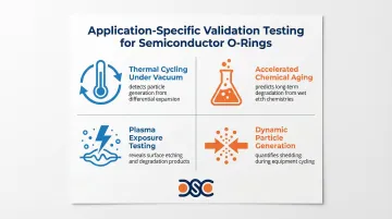
Application-Specific Validation
Standard ASTM E595 testing at 125°C doesn't replicate all semiconductor process conditions. Application-specific validation is recommended when process conditions differ from standard isothermal parameters:
- Thermal cycling under vacuum: Repeated heating/cooling cycles can cause particle generation from differential thermal expansion not detected in isothermal testing
- Accelerated aging in process chemicals: Exposure to actual wet etch chemistries or cleaning solutions at elevated temperature predicts long-term degradation
- Plasma exposure testing: RF plasma with actual process gases reveals surface etching and degradation product formation
- Particle generation under dynamic conditions: Simulated seal compression/decompression cycles quantify particle shedding during equipment cycling
Each of these tests targets a failure mode that standard screening won't catch — making them worth running before O-rings are qualified for a new process chamber or chemistry.
Common Specification Errors and Misinterpretations
Semiconductor O-ring specifications fail in predictable ways. These are the five most common errors — and what each one actually costs you.
Accepting NASA certification without checking TML/CVCM values. The standard allows up to 1.0% TML, but materials achieving 0.3% carry meaningfully lower contamination risk. Both technically "pass" — the gap in real-world performance is significant.
Specifying base polymer only. Writing "FFKM" on a drawing without designating a low-outgassing grade or cleanroom processing requirement leaves the door open for non-compliant substitutions. General-purpose FFKM for chemical processing uses different cure systems and fillers than semiconductor-grade material. Formulation and processing choices directly affect purity.
Focusing on outgassing while ignoring particle generation. Volatile and particulate contamination are separate pathways — and particulates often pose equal or greater risk. A material with excellent outgassing numbers but poor abrasion resistance still causes yield loss.
Applying industrial O-ring specs to cleanroom applications. Industrial specifications address dimensional tolerances and mechanical properties. They don't touch cleanroom manufacturing conditions, DI water cleaning protocols, or the purity documentation semiconductor applications require.
Defaulting to FFKM across the board. FFKM is the right choice where chemical resistance or thermal performance demands it — not everywhere. Properly formulated low-outgassing FKM or silicone meets requirements for many non-critical applications at 5–10% of FFKM cost. Reserve FFKM for applications where its unique properties are actually required.
Conclusion
Outgassing and material purity govern semiconductor cleanroom O-ring performance as active contamination pathways with direct consequences for process yield and equipment reliability. Volatile compounds deposit on wafers and create defects; particles contaminate cleanrooms; degradation products compromise process chemistry.
Effective O-ring selection requires understanding the full contamination pathway — from material formulation through application conditions. Specifications must address each stage:
- Material formulation: baseline purity and ASTM E595 outgassing limits
- Manufacturing environment: cleanroom classification to prevent surface contamination
- Cleaning protocols: DI water and validated residue removal procedures
- Application validation: testing under real process conditions to confirm long-term behavior
Published test data is a starting point — translating specifications into actual contamination control takes supplier expertise and application-specific validation. Detroit Sealing Components works with semiconductor customers across the full selection process, from material development through validation testing, backed by ISO 17025 accredited lab and ISO 9001:2015 certified quality system capabilities and cleanroom manufacturing experience.
Frequently Asked Questions
What is SEMI S2 S8 standard and how does it apply to O-rings?
SEMI S2 covers environmental, health, and safety guidelines for semiconductor equipment—including outgassing limits and contamination control—while SEMI S8 addresses ergonomic and safety design. Together, they shape O-ring material selection by defining the contamination thresholds and chemical compatibility requirements that prevent process failures.
What are the specifications for a cleanroom used to manufacture semiconductor O-rings?
Semiconductor-grade O-rings should be manufactured in ISO Class 5-7 cleanrooms (Class 100-10,000 per Fed Std 209) with controlled temperature, humidity, and particulate levels. Manufacturing is followed by DI water cleaning with resistivity >18 MΩ·cm, then double-bagging in a cleanroom environment to prevent contamination.
What is the best material for semiconductor cleanroom O-rings?
FFKM offers best overall performance—lowest outgassing, broadest chemical resistance, and highest temperature capability—for critical applications like plasma etch and CVD. Properly formulated low-outgassing FKM provides cost-effective performance for less demanding applications. Material selection depends on specific process conditions, contamination budget, and cost constraints.
What are the key specifications for semiconductor O-ring purity?
Key specs are TML <1.0% and CVCM <0.10% per ASTM E595 (stricter for ultra-high purity applications) and particle generation <100 particles >0.5μm/min. Additional requirements include low ionic and metal contamination, cleanroom manufacturing with DI water cleaning, and full material certification with lot traceability.
What is the ISO standard for O-rings used in semiconductor manufacturing?
O-ring dimensions follow ISO 3601 for size and tolerance. Semiconductor applications layer on ISO 14644 cleanroom classifications for the manufacturing environment and ASTM E595 for outgassing performance. SEMI standards (S2, S8) provide semiconductor-specific contamination and safety requirements.
How do you determine the right O-ring size for semiconductor equipment?
Start with ISO 3601 or AS568 gland design principles for static seals and Parker O-Ring Handbook guidelines for dynamic seals. Beyond standard sizing, semiconductor applications also demand low compression set to limit particle generation, allowances for thermal expansion during process cycling, and confirmed compatibility with vacuum and chemical exposure.